After half a day of soldering, the board looks like this:

Everything fits like a charm, and it really starts to look like a
Jupiter ACE. So it's time to start testing, and carefully insert all
chips.
Step 1: Check what is + and - on the power connector. It turns out
the Tip is ground, and the sleeve is +. Found myself a leftover power
supply (12VDC/1.4A) and mounted the 3.5 mm jack plug. Once connected
the LED goes green ! This is always a good start. After that I measured
the supply voltage on all main chips like the Z80 and some of the 74
series. All seems well.
So I first mount U23 74HC86, which is part of the oscillator, so now we should the 6.5 MHz on pin 8.
Which does not happen. There is a clear oscillator signal (with the right frequency) on pin 9, but its simply not big enough:

The signal gets bigger if I replace R2 with a 470K, just enough to get the signal on pin 8 going:

Still
looks a bit wacky, but I think that's also a limitation of my
oscilloscope which has a maximum sampling rate of 25 MHz so there are
only 4 samples per cycle.
Inserting U9: This is the clock signal divider, so there should be a clock on pin3 of U9:

Well,
at least it starts looking like a square wave now. So lets insert the
next two counters, U10 and U11. Which seems to work as well, so lets
mount all other chips. All good, until I came to inserting the RAM
chips:

OH
NO !! The footprint is wrong. It took me about half a second to realize
what was wrong: I selected the DIP28 footprint for this DIP24 chip. Not
something KiCad will warn you for, after all the DIP28 has plenty of
pins for a DIP24. After about 10 minute of quiet contemplation (...) I
decided that I would have to make some kind of adapter with 28 pins on
one side and a 24 pin socket on the other so I could re-route all pins
from 12 and up.
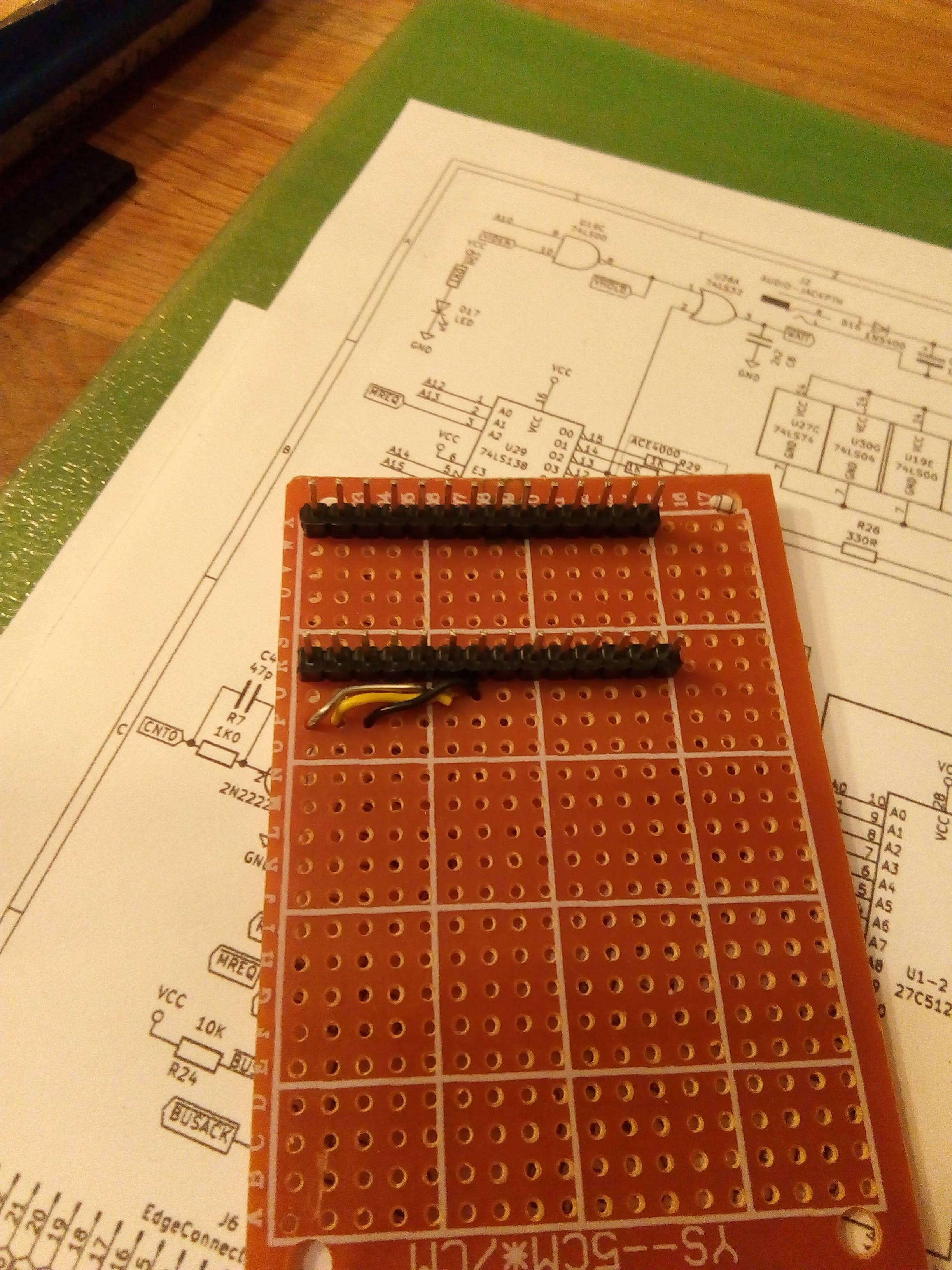
Good plan, but after struggling with the first four wires, and
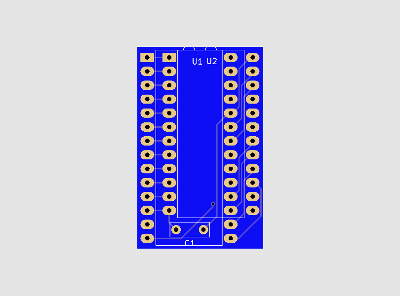
realizing I would have to do 3 adapters in total I gave up. Opened KiCad
again and designed an adapter PCB in about 30 minutes. Checked with the
PCB manufacturer and found that it would cost €19,- to have 15 pcs
manufactured.