After drawing the schematic and switching to the PCB design, the first thing I did was to arrange all components in a similar way as on the original board. Since I did follow the slightly modified version of the schematic with different memory chips, I had to make some changes, but overall the look is similar.
 |
| Original board layout, by Grant Searle |
 | |||||||
| Layout, and ratsnest lines |

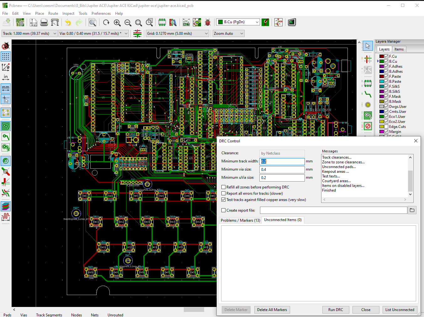
And so, after more than a year, (where I decided multiple times that it was just to hard and almost gave up), it is finally completely routed:
And since KiCad has a 3D display tool, I can now compare my version to the original:
